


Ya instalados los programas MPLAB y XC8, se explicará como crear un proyecto en MPLAB, configuración de registros o bits necesarios para el PIC18F4550 así como realizar un pequeño ejemplo de código de como encender y apagar el led RC1 que incorpora la tarjeta de desarrollo UNIT MICROPIC4550.
Por último se mencionará como compilar el código y dejarlo listo para después cargarlo mediante USB con el Software HIDBootloader si es que el PIC cuenta con el Bootloader USB, en caso de no tener el Bootloader cargado en el PIC tendrás el enlace para cargar los códigos con el programador PICKIT 3.
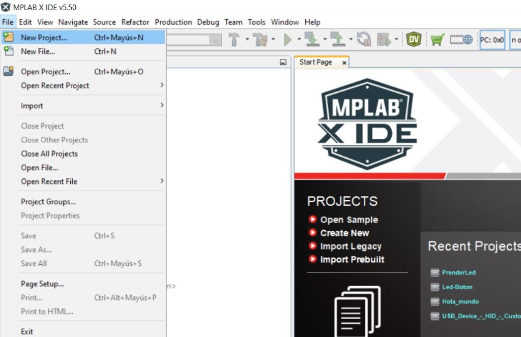
Sigue los siguientes pasos para crear tu primer proyecto en MPLAB.- Ejecuta MPLAB y selecciona del menú de la parte superior File -> New Project
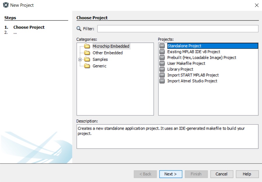
2. Saldrá la siguiente ventana, selecciona Microchip Embedded -> Standalone Project y da clic en Next.
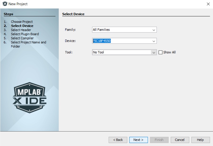
3. En la siguiente ventana, selecciona el PIC18F4550 te recomiendo escribir la matrícula directamente para evitar buscarlo en las lista de todos los microcontroladores, lo demás campos se quedan igual y presiona Next.
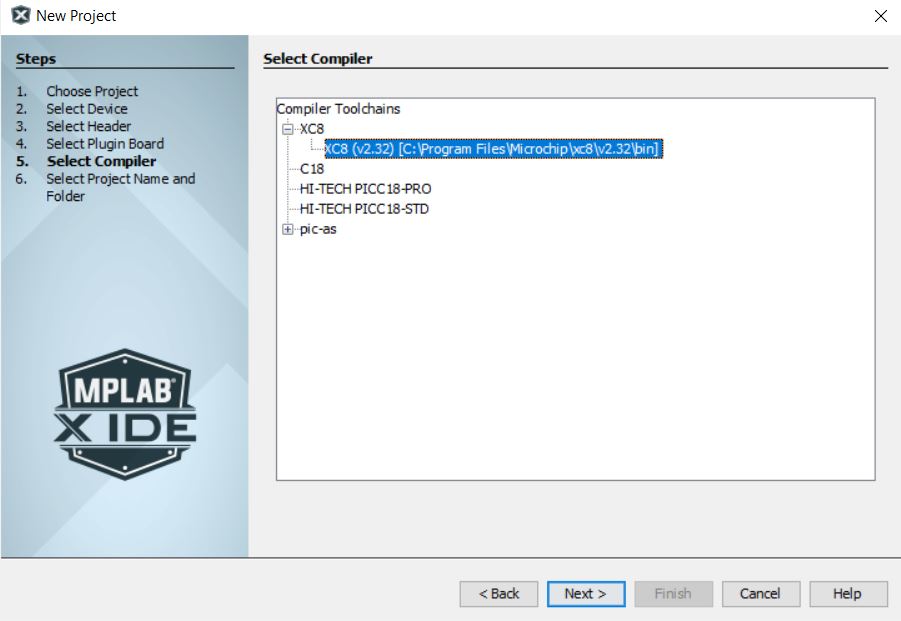
4. En la siguinte ventana selecciona el compilador XC8. Luego haz clic Next.
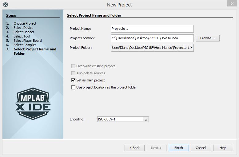
5. Asigna nombre al proyecto, por ejemplo “Hola Mundo”, después da clic en Browse, para guardar el proyecto en la ruta que requieras ya que después será importante conocer donde se guardo el proyecto para tener acceso rápido al .HEX, por último da clic en Finish.
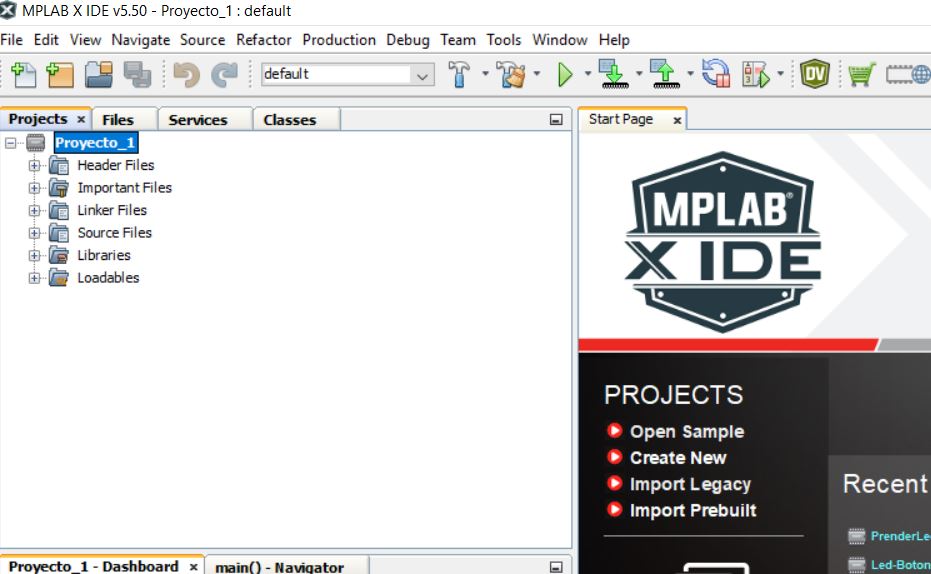
6. Ahora nuestro proyecto se muestra en la ventana Projects.
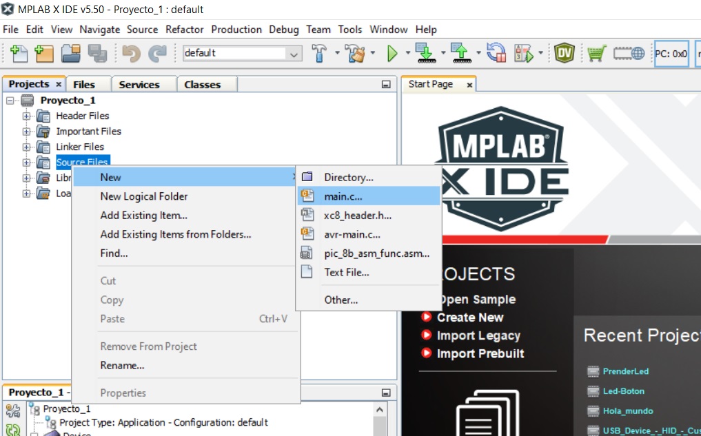
7. Ya hecho el proyecto deberás crear un nuevo archivo main.c, para hacerlo dirígete a Source Files, da clic derecho encima de esta opción, se desplegará una ventana, da clic en New y después en main.c Ahora nuestro proyecto se muestra en la ventana Projects.
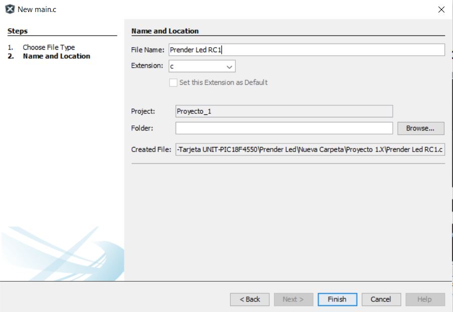
8. Dar nombre al archivo main.c y dar clic en Next.
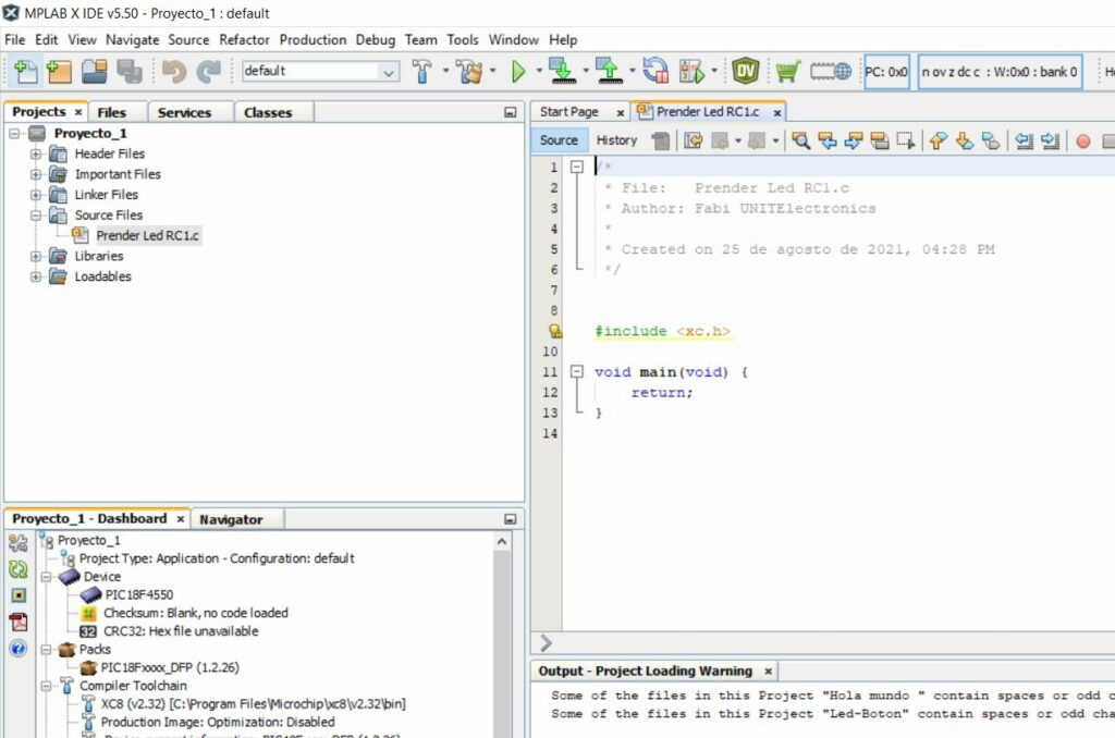
9. El proyecto queda de la siguiente y estará listo para realizar el código de encendido y apagado de los led´s que vienen incorporado a la tarjeta UNIT MICROPIC4550.
Configuración de registros para el PIC18F4550
El PIC18F4550 tiene registros de configuración, por lo que están configurados por defecto por el compilador, para evitar errores y problemas en los registros. Te recomiendo configurarlos antes de comenzar el código. Para configurar estos registros en MPLAB proporciona una forma simple de hacerlo, siguiente los pasos:
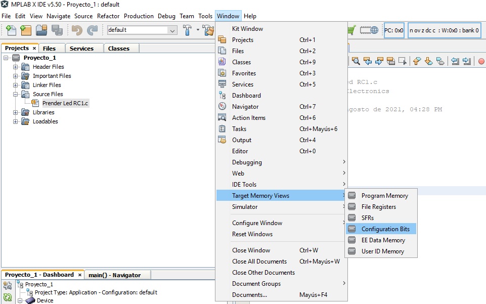
- Dirígete a las siguientes ventanas para entrar en “Configuration Bits“.
Window -> Target Memory Views -> Configuration Bits
2. Saldrá una venta debajo del código, da doble clic encima de la pestaña Configuration Bits como se muestran a continuación:
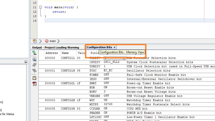
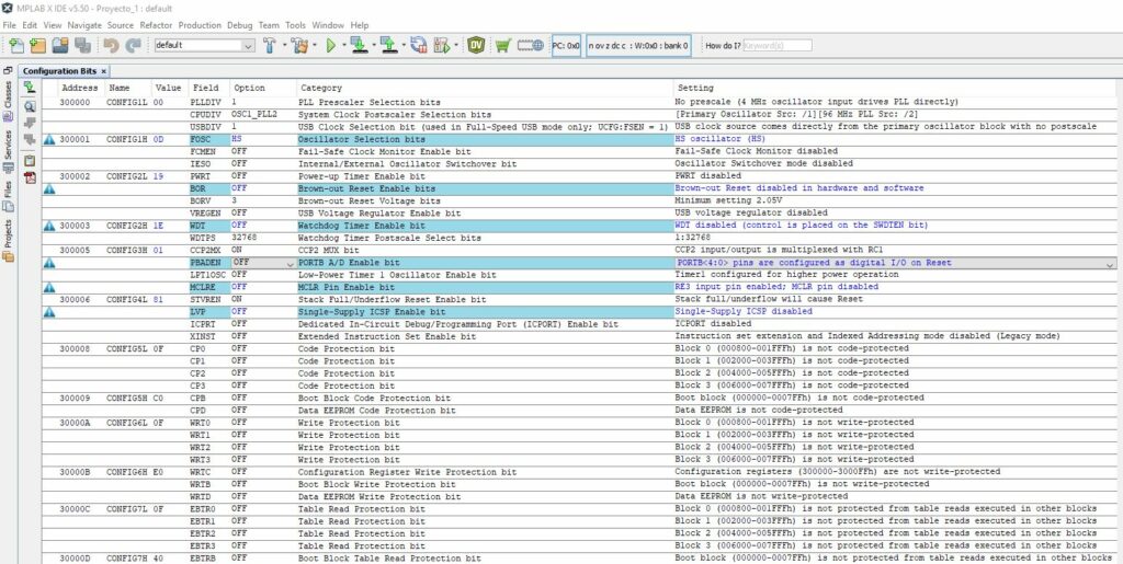
3. Se desplegará la ventana de Configuration Bits como se muestra a continuación:
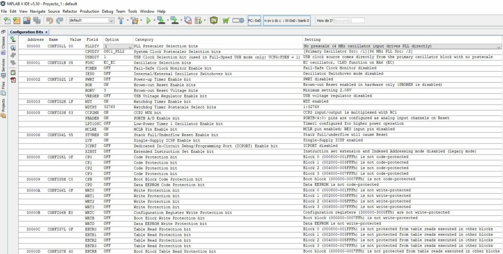
4. Cambia los siguientes registros como se muestra a continuación:
| Field | Option |
| FOSC | HS |
| BOR | OFF |
| WDT | OFF |
| MCLRE | OFF |
| PBADEN | OFF |
| LVP | OFF |
5. Quedará de la siguiente manera:
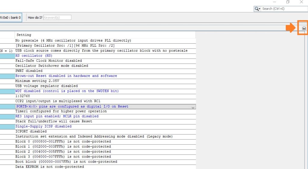
6. Presiona el botón Generate source Code to Output como se muestra a continuación.

7. Saldrá una venta en la parte inferior, deberás copiar el código que genero. En el siguiente código puedes checar un ejemplo:
// PIC18F4550 Configuration Bit Settings

// 'C' source line config statements

// CONFIG1L
#pragma config PLLDIV = 1       // PLL Prescaler Selection bits (No prescale (4 MHz oscillator input drives PLL directly))
#pragma config CPUDIV = OSC1_PLL2 // System Clock Postscaler Selection bits ([Primary Oscillator Src: /1][96 MHz PLL Src: /2])
#pragma config USBDIV = 1       // USB Clock Selection bit (used in Full-Speed USB mode only; UCFG:FSEN = 1) (USB clock source comes directly from the primary oscillator block with no postscale)

// CONFIG1H
#pragma config FOSC = HS        // Oscillator Selection bits (HS oscillator (HS))
#pragma config FCMEN = OFF      // Fail-Safe Clock Monitor Enable bit (Fail-Safe Clock Monitor disabled)
#pragma config IESO = OFF       // Internal/External Oscillator Switchover bit (Oscillator Switchover mode disabled)

// CONFIG2L
#pragma config PWRT = OFF       // Power-up Timer Enable bit (PWRT disabled)
#pragma config BOR = OFF        // Brown-out Reset Enable bits (Brown-out Reset disabled in hardware and software)
#pragma config BORV = 3         // Brown-out Reset Voltage bits (Minimum setting 2.05V)
#pragma config VREGEN = OFF     // USB Voltage Regulator Enable bit (USB voltage regulator disabled)

// CONFIG2H
#pragma config WDT = OFF        // Watchdog Timer Enable bit (WDT disabled (control is placed on the SWDTEN bit))
#pragma config WDTPS = 32768    // Watchdog Timer Postscale Select bits (1:32768)

// CONFIG3H
#pragma config CCP2MX = ON      // CCP2 MUX bit (CCP2 input/output is multiplexed with RC1)
#pragma config PBADEN = OFF     // PORTB A/D Enable bit (PORTB<4:0> pins are configured as digital I/O on Reset)
#pragma config LPT1OSC = OFF    // Low-Power Timer 1 Oscillator Enable bit (Timer1 configured for higher power operation)
#pragma config MCLRE = OFF      // MCLR Pin Enable bit (RE3 input pin enabled; MCLR pin disabled)

// CONFIG4L
#pragma config STVREN = ON      // Stack Full/Underflow Reset Enable bit (Stack full/underflow will cause Reset)
#pragma config LVP = ON         // Single-Supply ICSP Enable bit (Single-Supply ICSP enabled)
#pragma config ICPRT = OFF      // Dedicated In-Circuit Debug/Programming Port (ICPORT) Enable bit (ICPORT disabled)
#pragma config XINST = OFF      // Extended Instruction Set Enable bit (Instruction set extension and Indexed Addressing mode disabled (Legacy mode))

// CONFIG5L
#pragma config CP0 = OFF        // Code Protection bit (Block 0 (000800-001FFFh) is not code-protected)
#pragma config CP1 = OFF        // Code Protection bit (Block 1 (002000-003FFFh) is not code-protected)
#pragma config CP2 = OFF        // Code Protection bit (Block 2 (004000-005FFFh) is not code-protected)
#pragma config CP3 = OFF        // Code Protection bit (Block 3 (006000-007FFFh) is not code-protected)

// CONFIG5H
#pragma config CPB = OFF        // Boot Block Code Protection bit (Boot block (000000-0007FFh) is not code-protected)
#pragma config CPD = OFF        // Data EEPROM Code Protection bit (Data EEPROM is not code-protected)

// CONFIG6L
#pragma config WRT0 = OFF       // Write Protection bit (Block 0 (000800-001FFFh) is not write-protected)
#pragma config WRT1 = OFF       // Write Protection bit (Block 1 (002000-003FFFh) is not write-protected)
#pragma config WRT2 = OFF       // Write Protection bit (Block 2 (004000-005FFFh) is not write-protected)
#pragma config WRT3 = OFF       // Write Protection bit (Block 3 (006000-007FFFh) is not write-protected)

// CONFIG6H
#pragma config WRTC = OFF       // Configuration Register Write Protection bit (Configuration registers (300000-3000FFh) are not write-protected)
#pragma config WRTB = OFF       // Boot Block Write Protection bit (Boot block (000000-0007FFh) is not write-protected)
#pragma config WRTD = OFF       // Data EEPROM Write Protection bit (Data EEPROM is not write-protected)

// CONFIG7L
#pragma config EBTR0 = OFF      // Table Read Protection bit (Block 0 (000800-001FFFh) is not protected from table reads executed in other blocks)
#pragma config EBTR1 = OFF      // Table Read Protection bit (Block 1 (002000-003FFFh) is not protected from table reads executed in other blocks)
#pragma config EBTR2 = OFF      // Table Read Protection bit (Block 2 (004000-005FFFh) is not protected from table reads executed in other blocks)
#pragma config EBTR3 = OFF      // Table Read Protection bit (Block 3 (006000-007FFFh) is not protected from table reads executed in other blocks)

// CONFIG7H
#pragma config EBTRB = OFF      // Boot Block Table Read Protection bit (Boot block (000000-0007FFh) is not protected from table reads executed in other blocks)
9. Para salir de la venta de Generate source Code to Output da clic como se muestra a continuación:
Se mostrará la siguiente pantalla:
10. En la parte superior del código deberás pegar el código generado en la configuración de los registros. En el siguiente código se muestra como debe quedar:
// PIC18F4550 Configuration Bit Settings
// 'C' source line config statements
// CONFIG1L
#pragma config PLLDIV = 1 // PLL Prescaler Selection bits (No prescale (4 MHz oscillator input drives PLL directly))
#pragma config CPUDIV = OSC1_PLL2 // System Clock Postscaler Selection bits ([Primary Oscillator Src: /1][96 MHz PLL Src: /2])
#pragma config USBDIV = 1 // USB Clock Selection bit (used in Full-Speed USB mode only; UCFG:FSEN = 1) (USB clock source comes directly from the primary oscillator block with no postscale)
// CONFIG1H
#pragma config FOSC = HS // Oscillator Selection bits (HS oscillator (HS))
#pragma config FCMEN = OFF // Fail-Safe Clock Monitor Enable bit (Fail-Safe Clock Monitor disabled)
#pragma config IESO = OFF // Internal/External Oscillator Switchover bit (Oscillator Switchover mode disabled)
// CONFIG2L
#pragma config PWRT = OFF // Power-up Timer Enable bit (PWRT disabled)
#pragma config BOR = OFF // Brown-out Reset Enable bits (Brown-out Reset disabled in hardware and software)
#pragma config BORV = 3 // Brown-out Reset Voltage bits (Minimum setting 2.05V)
#pragma config VREGEN = OFF // USB Voltage Regulator Enable bit (USB voltage regulator disabled)
// CONFIG2H
#pragma config WDT = OFF // Watchdog Timer Enable bit (WDT disabled (control is placed on the SWDTEN bit))
#pragma config WDTPS = 32768 // Watchdog Timer Postscale Select bits (1:32768)
// CONFIG3H
#pragma config CCP2MX = ON // CCP2 MUX bit (CCP2 input/output is multiplexed with RC1)
#pragma config PBADEN = OFF // PORTB A/D Enable bit (PORTB<4:0> pins are configured as digital I/O on Reset)
#pragma config LPT1OSC = OFF // Low-Power Timer 1 Oscillator Enable bit (Timer1 configured for higher power operation)
#pragma config MCLRE = OFF // MCLR Pin Enable bit (RE3 input pin enabled; MCLR pin disabled)
// CONFIG4L
#pragma config STVREN = ON // Stack Full/Underflow Reset Enable bit (Stack full/underflow will cause Reset)
#pragma config LVP = ON // Single-Supply ICSP Enable bit (Single-Supply ICSP enabled)
#pragma config ICPRT = OFF // Dedicated In-Circuit Debug/Programming Port (ICPORT) Enable bit (ICPORT disabled)
#pragma config XINST = OFF // Extended Instruction Set Enable bit (Instruction set extension and Indexed Addressing mode disabled (Legacy mode))
// CONFIG5L
#pragma config CP0 = OFF // Code Protection bit (Block 0 (000800-001FFFh) is not code-protected)
#pragma config CP1 = OFF // Code Protection bit (Block 1 (002000-003FFFh) is not code-protected)
#pragma config CP2 = OFF // Code Protection bit (Block 2 (004000-005FFFh) is not code-protected)
#pragma config CP3 = OFF // Code Protection bit (Block 3 (006000-007FFFh) is not code-protected)
// CONFIG5H
#pragma config CPB = OFF // Boot Block Code Protection bit (Boot block (000000-0007FFh) is not code-protected)
#pragma config CPD = OFF // Data EEPROM Code Protection bit (Data EEPROM is not code-protected)
// CONFIG6L
#pragma config WRT0 = OFF // Write Protection bit (Block 0 (000800-001FFFh) is not write-protected)
#pragma config WRT1 = OFF // Write Protection bit (Block 1 (002000-003FFFh) is not write-protected)
#pragma config WRT2 = OFF // Write Protection bit (Block 2 (004000-005FFFh) is not write-protected)
#pragma config WRT3 = OFF // Write Protection bit (Block 3 (006000-007FFFh) is not write-protected)
// CONFIG6H
#pragma config WRTC = OFF // Configuration Register Write Protection bit (Configuration registers (300000-3000FFh) are not write-protected)
#pragma config WRTB = OFF // Boot Block Write Protection bit (Boot block (000000-0007FFh) is not write-protected)
#pragma config WRTD = OFF // Data EEPROM Write Protection bit (Data EEPROM is not write-protected)
// CONFIG7L
#pragma config EBTR0 = OFF // Table Read Protection bit (Block 0 (000800-001FFFh) is not protected from table reads executed in other blocks)
#pragma config EBTR1 = OFF // Table Read Protection bit (Block 1 (002000-003FFFh) is not protected from table reads executed in other blocks)
#pragma config EBTR2 = OFF // Table Read Protection bit (Block 2 (004000-005FFFh) is not protected from table reads executed in other blocks)
#pragma config EBTR3 = OFF // Table Read Protection bit (Block 3 (006000-007FFFh) is not protected from table reads executed in other blocks)
// CONFIG7H
#pragma config EBTRB = OFF // Boot Block Table Read Protection bit (Boot block (000000-0007FFh) is not protected from table reads executed in other blocks)
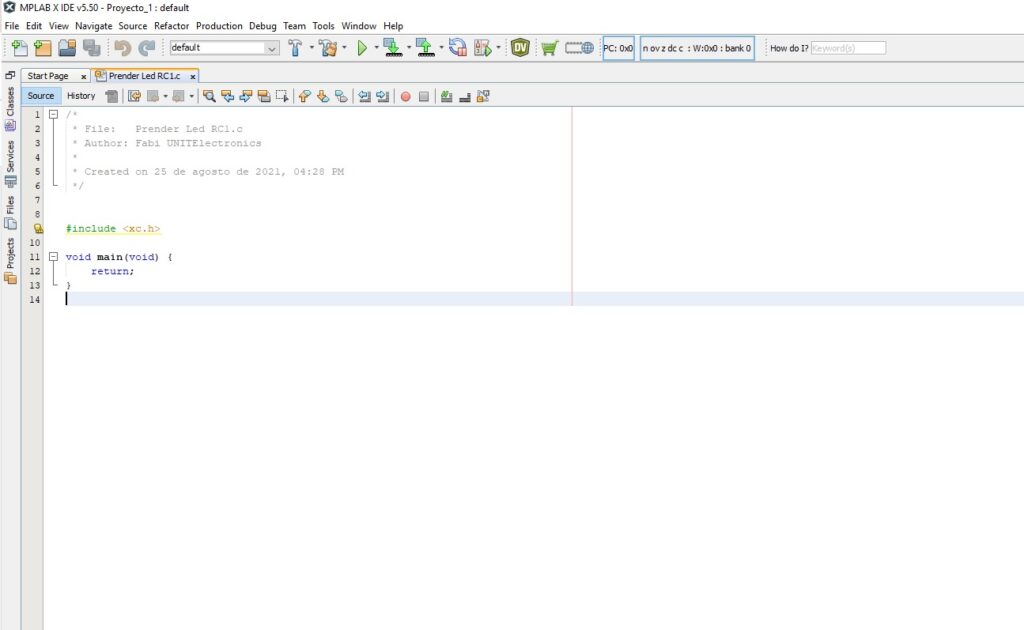
#include <xc.h> // Biblioteca para el compilador XC8
void main(void) {
return;
}
Video de apoyo, para configurar los registros y dejar preparado el código en C
11. Agregar las siguientes líneas de código.
#include <stdlib.h> //Biblioteca para declarar funciones y utilizar cadenas de caracteres
#include <stdio.h> //Biblioteca para definir Entradas / Salidas
#define _XTAL_FREQ 20000000 //Define la frecuencia del oscilador de la placa, así como los micro __delay(_ms) o __delay_us()

void main(void) {
    TRISC = 0x00; // 0-> salida, 1-> entrada, Establece la dirección de PORTC como SALIDA a la que se conecta el LED

    while(1){
        PORTCbits.RC1 = 1; //Se define que el pin RC1 este en ALTO
         __delay_ms (500); //Se mantienen en ALTO por 500ms
        PORTCbits.RC1 = 0; //Se define que el pin RC1 este en BAJO
        __delay_ms (500); //Se mantienen en BAJO por 500ms
    }
    return; //Reanuda la función
}
13. Por último compila el código como se muestra en el siguiente vídeo.
Consulta el siguiente video el cual se explica el funcionamiento de MICROPIC4550 y como cargar el .Hex mediante el puerto USB con ayuda del programa HIDBootloader
Consulta el siguiente tutorial para Programar UNIT MICROPIC4550 con PICKIT 3 y carga el .HEX generado con el proyecto anteriormente explicado.


